Initiate develpment of ultra fine processing in nano meter level
―Aim to create new businesses with new surface structures applying high precision optical elements and biomimetics―
What is Ultra precision fine surface processing?
At Nalux, we develop and manufacture optical components with nanometer-scale microstructures by applying lithography techniques derived from semiconductor manufacturing. Below is an overview of the standard fabrication process.

1. Photoresist Coating
A photosensitive resin (photoresist) is dispensed onto the surface of a substrate such as silicon or quartz glass. The substrate is then spun at high speed using a spin coater, allowing centrifugal force to spread the resist into a uniform thin film.
2. Exposure
Ultraviolet (UV) light is projected onto the photoresist through a photomask containing fine patterns. The exposed areas undergo chemical changes, transferring the mask pattern onto the resist layer.
Nalux also supports electron beam lithography for achieving finer structures, as well as laser patterning for creating three-dimensional features.
3. Development
The exposed, unnecessary portions of the photoresist are dissolved and removed using a dedicated developer solution. This process forms a resist pattern on the substrate, protecting areas that should remain intact during the subsequent etching step.
4. Etching
Using a dry etching system with reactive gases such as plasma, the areas of the substrate not protected by the resist are selectively removed. By employing anisotropic etching with high vertical precision, sharp, high-aspect-ratio microstructures can be achieved.
5. Resist Stripping
After processing, the remaining photoresist is completely removed using oxygen plasma (ashing) or specialized stripping solutions.
6. Final Product
The desired microstructures are formed on the substrate surface, completing the process.
By repeating steps 1 through 6, complex multi-step structures can be fabricated. The substrate may then be diced into individual components, and additional treatments such as anti-reflective coating may also be applied as required. Final inspection and quality assurance are performed prior to shipment.
Nalux's Lithography technologies
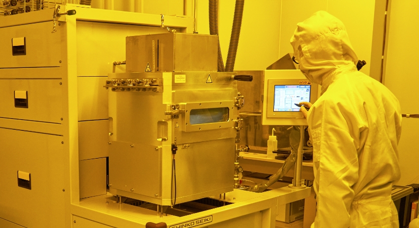
Nalux has been working hard on R&D of ultra fine surface procesing best utilizing various equipments such as Nalux's own in-house lithography equipment and also external semiconductor processing equipments available at Fine Processing Platform of Center for Integrated Nano Technology Support located in Tohoku Univ.
Nalux is aiming to develop new businesses by R&D works applying biomimetics which is copying surface structures of living things, enabling to provide surface characteristics such as Anti-reflection and Water repellency function.
At Nalux, we also offer contract manufacturing services for microstructures. By leveraging the know-how we have developed over the years, we assist in turning your ideas into reality. We provide comprehensive and integrated solutions—from designing or prototyping new microstructures, to evaluating their dimensional accuracy or optical performance, all under a unified development framework.
Please feel free to reach out to us. → Inquiries
Examples of lithography process
Photoresist patterning
- Exposure with Photo mask
- Laser Drawing
- Electron beam drawing
Shape transfer
- UV imprint
- Electroforming
Etching
- Plasma etching
- Wet etching
Thin film formation
- Spattering
- Lift-off process
Metalenses
A metalens is a flat lens that manipulates light using subwavelength-scale nanostructures, known as meta-atoms, formed on its surface. Unlike conventional lenses, metalenses enable various functionalities such as polarization control and wavelength separation, making it possible to achieve not only a thinner profile but also enhanced multi-functionality. At Nalux, we utilize our expertise in optical design and ultra-fine processing technologies to develop and prototype metalenses. As a result, we have achieved optical performance closely aligned with theoretical design values.
Whether you need only design, only prototyping, or full support from design through fabrication and evaluation, Nalux is ready to meet a broad range of customer needs.
Prototype Design Values and Evaluation Results
| Item | Design Values | Measured Values |
| Wavelength | 8-14 μm | |
| Material | Si | |
| Effective Size | 7 mm × 7 mm | |
| Thickness | 0.5 mm | |
| F-number | 1.84 | Approx. 1.8 |
| Horizontal Field of View | 17° | 17° |
| Center CTF (11 lp/mm) |
Approx. 20% | Approx. 15% |

Random Phase Plate
A random phase plate is an optical element that features a random structure (random binary array) on its surface, with appropriate size and depth. Random phase plate introduces controlled phase differences into the wavefront of the transmitted light beam, shaping the focal spot into a Gaussian distribution. Compared to conventional spatial filters that utilize lenses and pinholes, the random phase plate offers higher efficiency. Furthermore, beam quality control through the pixel size of the random phase plate has been reported in processing that using excimer lasers with complex transverse modes.
Konda et al., "Measurement of the Excimer-Laser Ablation Threshold Using the Random Phase Plate," 2024 Conference on Lasers and Electro-Optics Pacific Rim (CLEO-PR), Incheon, Korea, Republic of, 2024, pp. 1-5
At Nalux, we support not only simple two-level random phase plates but also multi-step random phase plates with multiple phase level.

Volume Binary Grating (VB grating)
The Volume Binary grating (VB grating) is a transmissive diffraction grating that offers high diffraction efficiency and large angular dispersion across a broad bandwidth. It is gaining attention as a novel dispersive optical element for next-generation large space telescopes. The VB grating features a rectangular structure with a high aspect ratio. While anisotropic etching using reactive gases typically degrades sidewall verticality and bottom flatness as processing progresses, Nalux minimizes these effects through optimized processing conditions, enabling the fabrication of high-precision rectangular structures.
Nalux manufactured quartz-based VB gratings for a collaborative project involving the Japan Aerospace Exploration Agency (JAXA), Osaka University (currently Ritsumeikan University), and the RIKEN Center for Advanced Photonics (RAP).
N. Ebizuka et al., "Novel gratings for astronomical observations II," Proceedings Volume 11852, International Conference on Space Optics — ICSO 2020; 1185263 (2021)
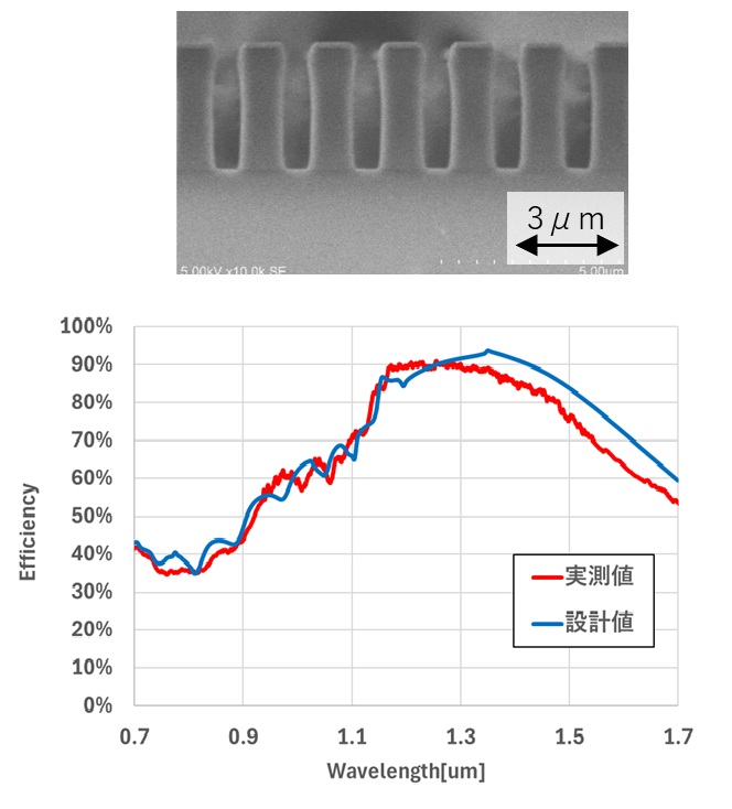
Bottom: VB Grating Design and Measured Results
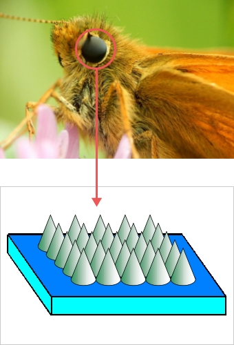
ARS(ARS:Anti-Reflective Structure)
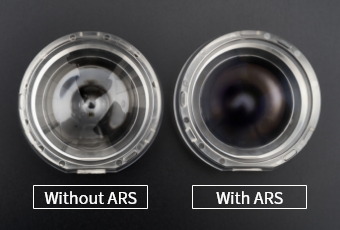
Moth eye has very fine peaks and troughs structures which have functions to suppress reflection of light. Thus structure is called ARS (Anti Reflection Structure). Conventional method to achieve anti-reflection function on optical part is to apply coating by vacuum deposition, while ARS generated by fine surface processing has advantages such as low incident angle dependence of light, no delamination or cracks of coating in principle and applicable even for the poor coating adhesion lmaterials like PMMA.
Nalux has been working on developing process technologies of creating ARS on lens surface.
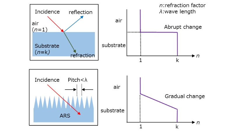
How it works.
Reflection of light is caused by drastic change of refractive index, for example when light enters lens from air. Reflection of light is suppressed when lens has structures which are smaller pitches than wave length of light on its surface, because those structures help to make refractive index change smoother.
Nalux's ARS characteristics
- Improved shape transfer of moth eye structures on lens by changing to concave profile from convex one (US Patent No.11/921,324 granted)
- Unique processing (PAT 5584907 granated) which enables to tranfer moth eye structure on curved and large area. Track record: 60mm diameter.
- Optimized structure design feasible by using Nalux's unique optical design software developed in house.
- RIE(Reactive Ion Etching) technology applicable for direct processing on lens (JP-Patent No. 6611113, No. 6901189).
RIE application and processing examples
- Suitable for illumination lens used under direct sunshine and automobile applications requirng high reliability;
- Imaging and Sensor system
- Lens product which requires dust proof characteristic such as medical endoscopes
Application to optics having high dependency on incident angle of light :
Substrate materials: Silicon, Polycarbonate, Acrylic, Fused silica, etc.
Our track records on various materials:
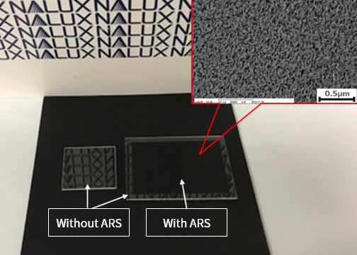
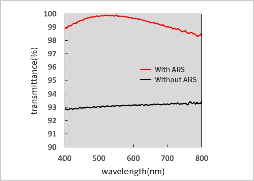
ARS processing example on fused silica:
You see no reflection on fused silica with ARS on the right while you see reflection of "Letters on the wall" on the fused silica without ARS on the left.
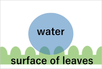
Ultra hydrophobicity property (water repellency) achieved by using the ARS
Technology to generate fine structures like ARS on the lens surface is applicable to control wettability of the material surfaces. It is widely known that lotus has water repellent leaves , so called "lotus effect" in nature. This effect is achieved because concave and convex structures on the leaf surface enhance water repellency or hydrophobicity.
We can thus control wettability by fine structures taking advantage of lotus leaf effect.
One advantage is that we can provide hydrophobicity property by etching process direct on lens surfaces to materials not suitable for conventional water repellency process such as vacuum deposition or spraying. Another advantage is to provide antifouling effect on the lens.

Other application example: Black Silicon
Hydrophobic property becomes much stronger if water repelency coating is done on substrate having micro fine structure rather than a flat smooth substrate.
At Nalux, we achieved remarkably large contact angle of over 160 degrees(In general contact angle over 150degree is called "Ultra water repellent status".